Previously, it was possible to distinguish the left-right rotational light only by using complex filters or organic sensitive materials, but KAIST researchers succeeded in developing a polarization detection sensor that selectively responds well to Circularly Polarized Light (CPL) in a specific direction without complex devices.
KAIST announced on the 28th that a research team led by Professor Jihyeon Yeom of the Department of Materials Science and Engineering has successfully developed the first wideband circular polarization (CPL) detection semiconductor material that can detect ultraviolet to short-wavelength infrared rays using atomic-level chiral control of selenium.
This innovative technology is a film-type material that can detect circular polarization (CPL) at room temperature with high sensitivity. It is attracting attention as a key material for quantum computing, spintronics, and photosensor technology, such as decoding light-encrypted information or controlling quantum bits.
Chirality refers to left-right asymmetry and is a very important physical property not only at the molecular level but also throughout optics, medicine, and life phenomena. It is a technology to distinguish circular polarization (CPL), which is important for detecting the spin characteristics of light.
Mindful of the fact that CPL sensors are vulnerable to moisture or ultraviolet rays and are prone to deterioration, Professor Jihyeon Yeom ’s team turned their attention to selenium (Se)—an inorganic material known for its inherent chiral crystal structure and long-term stability.
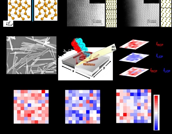
Selenium has a unique chiral structure and can increase performance stability semi-permanently. However, the atomic structure naturally exists in both right and left directions, making it challenging to control in one direction and limiting its practical use. The research team developed a ‘chiral transfer technology’ that can control the lattice structure to have asymmetry (chirality) in the left or right direction by making selenium (Se) into a ‘selenium nanorod’ in the form of a nano-sized rod.
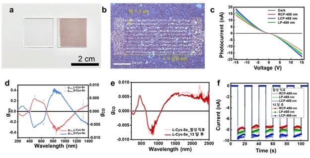
The researchers confirmed that the manufactured selenium nanofilm device can detect CPL in a wide wavelength range from ultraviolet rays (180 nm) to short-wavelength infrared rays (2500 nm), and recorded excellent performance in precisely distinguishing polarization directions without additional polarization filters, with a light response asymmetry index of up to 0.4 (0 being unable to distinguish left and right light at all, ±0.1 being fine distinguishable, and ±0.4 being recognized as a high-performance sensor because it can distinguish abnormal left/right circular polarization very clearly).
Importantly, the Se nanofilm maintained its performance without any degradation for over 13 months in ambient conditions, showcasing its long-term operational stability—a key advantage of using an inorganic material platform.
In the past, lattice chirality could be analyzed through expensive transmission electron microscope (TEM) equipment, while the newly developed 2D Raman photoactivity (2D ROA) mapping technique is a new and powerful analysis technology that can visualize and quantitatively analyze how the chiral structure (left/right asymmetry) of selenium nanofilm is distributed throughout the film.
Professor Jihyeon Yeom of the Department of Materials Science and Engineering at KAIST stated, “This study presents a new methodology for implementing and analyzing chiral properties in the field of semiconductor optical materials. As it can selectively read and distinguish circular polarization information of light, it can be applied to light-based quantum information processing or developing low-power semiconductor technology. The selenium nanofilm synthesis process used in this study takes place at room temperature, and it is an eco-friendly process that does not require harmful chemicals or high-temperature heat treatment and can be safely tested at room temperature.”
She also emphasized that “We will be able to expand to base technologies that can be applied to various fields such as quantum optics, security optics, bio-diagnosis, and image sensors.”
The research was conducted in collaboration with Professor Kyung Min Kim’s team at the Department of Materials Science and Engineering of KAIST and led by Dr. Junyoung Kwon, currently an assistant professor at the Department of Nanotechnology Engineering of Pukyong National University, and a former postdoctoral researcher at KAIST. The findings were published on the 3rd in the prestigious journal Nature Communications under the title: “Enantioselective Se lattices for stable chiroptoelectronic processing media.”